
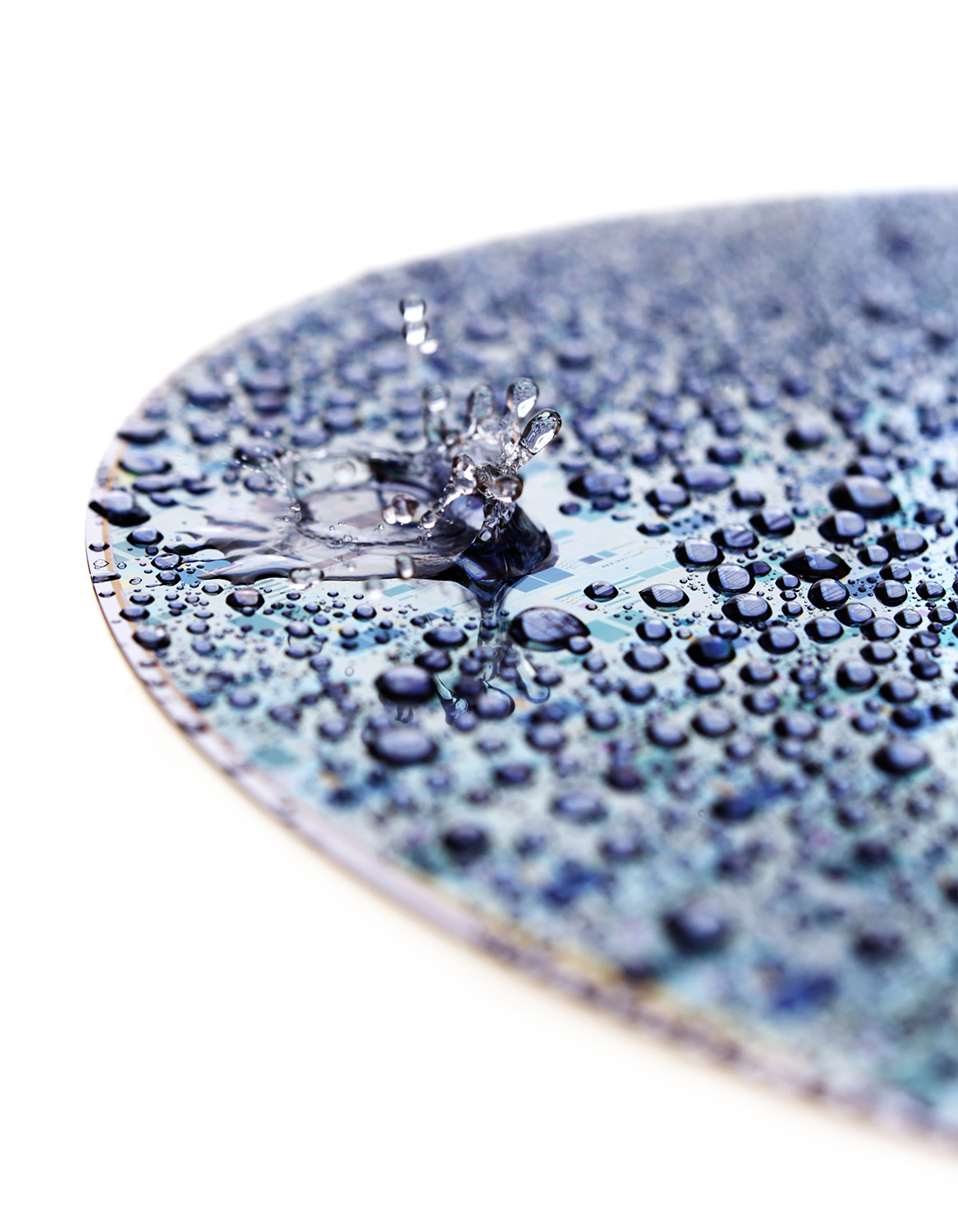
Material Level Innovation for Breakthrough Performance
WWe collaborate with partners worldwide to specify the very best materials, technologies, and processes to help optimize production, drive down costs and reduce risks inherent in electronics design and manufacturing.
Material Level Innovation for Breakthrough Performance
We collaborate with partners worldwide to specify the very best materials, technologies, and processes to help optimize production, drive down costs and reduce risks inherent in electronics design and manufacturing.
Material Level Innovation for Breakthrough Performance
Material Level Innovation for Breakthrough Performance
We collaborate with partners worldwide to specify the very best materials, technologies, and processes to help optimize production, drive down costs and reduce risks inherent in electronics design and manufacturing.

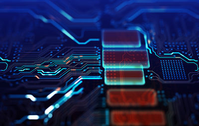
Semiconductor
Products

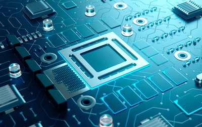
Semiconductor
Services

Collaboration
& Partnership
Research &
Development

Global
Reach
KAITEKI
Our Sustainability
Values
End-to-End Semiconductor Manufacturing Solutions and Services

Semiconductor Portfolio
- About Our Portfolio
- Front-End Solutions
- Back-End Solutions
- Power Electronics


GaN Substrate
With uniform and high-grade crystallinity and surface quality, the Mitsubishi Chemical Group’s high-quality material, allowing GaN devices on GaN substrate, contributes to the improved performance of laser diodes and power semiconductors at the mass production scale.
High-density proprietary BN fillers enhance thermal conductivity to 16.5W/mK in a resin sheet. Employing high-purity epoxy resin as a binder, it's ideal for power modules in inverters, converters, and on-board chargers. This sheet delivers thermal conduction, insulation, and adhesion in one.
Semiconductor Services
What we Offer
- Microparticle Eradication: Say goodbye to dust sources as our washing technology banishes minuscule particles from part surfaces.
- Altered Layer Removal: We delicately strip away fluoridated layers from ceramic-sprayed and metal surfaces without compromising roughness, minimizing particulate contamination.
- Polishing Material Elimination: We leave no remnants behind, completely removing polishing materials post-blast processing.
- Super-Clean Surfaces: Elevate your product quality with our supply of super-clean surfaces, meticulously purged of impurities for unparalleled value.
- Metal Contamination Reduction: Boost your yields by reducing metal contamination to unprecedented parts-per-trillion levels, backed by our in-house contamination analysis expertise.
Wafer Reclaiming
Revolutionizing Semiconductor Recycling: Our Solution in Action
- High-Quality Reclaimed Wafers for Cost-Efficient Production Unlock substantial cost savings with Shinryo's high-quality reclaimed wafers, crafted using our proprietary film removal and polishing technologies. Our expertise extends beyond mere recycling; we empower customers to maximize the reuse of wafers while ensuring swift order fulfillment.
- Efficient Reuse of Monitor and Dummy Wafers Streamline your semiconductor processes with our comprehensive solution for monitor and dummy wafers. We accept used wafers from customers, employing meticulous film-stripping, surface-polishing, and final cleaning processes to transform them into reusable products.
Why Shinryo
- Expertise: With our deep understanding of semiconductor and flat-panel display manufacturing, we're your trusted partner in precision cleaning solutions.
- Innovation: Stay ahead of the curve with our commitment to leveraging advanced cleaning and surface modification technologies.
- Results: Witness tangible improvements in yields and cost-effectiveness, empowering your business to thrive in the competitive landscape.
Ready to revolutionize your manufacturing processes? Take the first step towards unparalleled cleanliness and efficiency with Shinryo's Precision Cleaning Solutions!
Collaboration & Partnerships

We work together with engineers, OEMs, and businesses to help develop the right materials, designs, and processes to get ideas to market faster, cleaner, and more sustainably.
As a company that has the courage to break new ground, we’re proud to be part of a collaborative community of innovators that makes progress together by doing the right things for our people, society, and the environment.
Our vast network of expert teams and hands-on approach, from finding solutions to custom synthesis, mean we have real-world experience partnering with businesses across various industries, geographies, and applications.
“MCAM has consistently brought new innovative solutions to all segments of the Semiconductor industry, Port Plastics is a proud and long-term strategic supplier of MCAM materials in this critical industry”
~Scott Williams
Sr. Director, Industry Development
North American Plastics
“MCAM is a strategic partner for AMAT plastics business who provide excellence in vertical integration right from Raw Materials to finished goods.”
~Commodity Business Manager
World Wide Ops | Applied Materials, Inc.
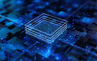
Research & Development
Gelest, Inc.
Advanced Materials
Polyester Film
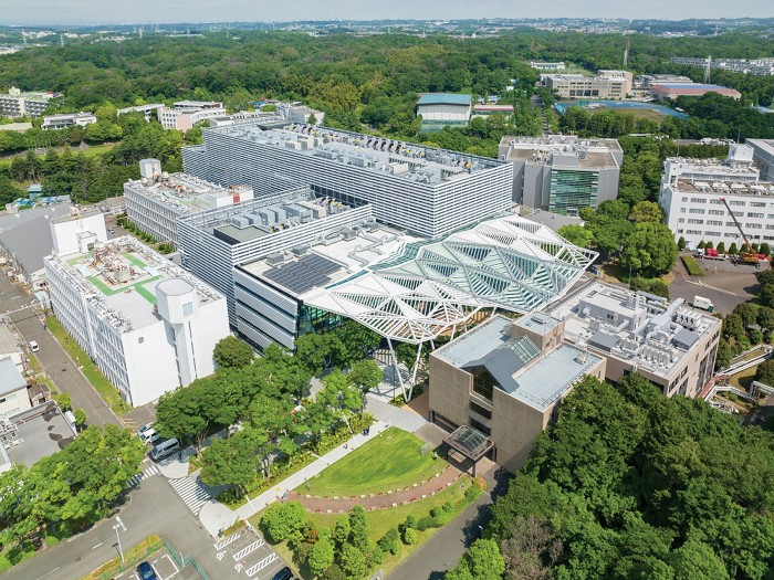
Embark on a journey of breakthroughs with our newly inaugurated Science & Innovation Center in Yokohama City, Japan. Spanning six stories and boasting a vast floor area of 42,000 m2, our state-of-the-art facility stands as a beacon of excellence in the semiconductor industry.
A Hub of Expertise and Collaboration
At our facility, we bring together the brightest minds from Mitsubishi Chemical Group, comprising top-notch R&D experts, scientists, and technology platform teams. From computational chemistry to analytical chemistry, our teams converge to pioneer environmentally friendly and innovative material technologies.
Fostering Global Partnerships
We open our doors to academia and venture companies worldwide, fostering collaborative environments where ideas flourish and solutions materialize. Together, we embark on a journey of discovery, pushing the boundaries of semiconductor materials to new heights.
Join us at the forefront of innovation as we redefine the possibilities of semiconductor materials at our cutting-edge Science & Innovation Center.
Global Footprint
The quickly-changing semiconductor market needs strong global partners with a sustained commitment to the industry. Mitsubishi Chemical Group is a truly global technology and manufacturing company. Our extensive knowledge in Chemical Science and our long-term strategy for further investments in material technologies positions us well to be a lasting partner.

KAITEKI Philosophy
Together, around 70,000 employees worldwide provide advanced chemistry-based solutions to deliver the core elements of our slogan - Science.Value.Life.
Mitsubishi Chemical Group's persistent determination to realize KAITEKI, our North Star, has guided our organization and its commitment to its stakeholders since 2011.


Contact us
Please select which region you would like to contact and fill in your details. We will be in touch as soon as possible.
Mitsubishi Chemical America
9115 Harris Corner Parkway
Charlotte, NC 28269

Copyright © Mitsubishi Chemical Group Corporation.